Laser Cut Alumina & Technical Ceramic Components
Applied Laser Solutions manufactures precision laser-cut, drilled, profiled and scribed ceramic components for thick film, thin film, microelectronics, engineering, aerospace, defence, medical and semiconductor applications.
We process 96% and 99% alumina, including common grades such as CoorsTek ADS-96R and CeramTec Rubalit 708S, with one-off, prototype and production quantities available.
Send us your CAD or DXF drawing, material, thickness, quantity and any tolerance or inspection requirements and we would be happy to provide a quote.
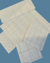
ceramic Substrates for Thick & Thin Film and hybrid circuit Applications
Laser scribed, drilled and profiled ceramic substrates for the micro-electronics, micro-hybrid, semiconductor, defence and aerospace industries.
Why laser? Most thick and thin film substrates are 96% alumina (Al₂O₃) which is extremely hard and not easily machinable so laser processing is the most efficient way to achieve clean features and tight repeatability.
Miniaturisation, one setup: Thick-film is a miniaturised process where a single substrate often carries many final circuits. With lasering, we scribe, profile, and drill in one setup:
Scribing: a line of laser pulses removes 30-50% of the material to create controlled break lines so panels snap cleanly into singles.
Drilling: produces vias between sides of the substrate.
Profiling: creates complex shapes in the ceramic.
Feature capability: Holes down to 0.06 mm are achievable (material-thickness dependent).
Common thicknesses: 96% alumina at 0.635 mm and 1.0 mm are typical; hybrid circuits are also produced from 0.254 mm up to 1.5 mm.
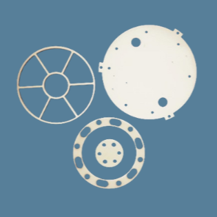
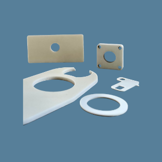
Laser-Cut Technical Ceramics for Engineering applications
Applied Laser Solutions manufactures precision laser-cut, drilled, profiled and scribed ceramic parts for thick film, thin film, microelectronics and engineering applications. We process 96% and 99% alumina, including common grades such as CoorsTek ADS-96R and CeramTec Rubalit 708S, with prototype, one-off and production quantities available.
Drilled and profiled parts for mechanical and engineering applications.
Design freedom: Laser cutting lets you design complex shapes with ease. 96% alumina is hard-wearing, and suitable for high-temperature applications:
Wear parts
Thermal management
Electrical management
You’ll find ceramic components across automotive, defence, medical, and even everyday household products.
Cost-effective at any scale: Lasering processing is economical because there no tooling charges when you order from us. This makesone-offs and prototypes viable as well as production quantities.
Workable tolerances of ±0.05 mm apply in most thicknesses.
Thick material capability: We cut alumina up to 4 mm thick (stock up to 3 mm).
File formats: CAD/CAM drawings accepted in DXF.
Materials & Grades
Alumina 96% & 99% for thickand thin film and engineering applications
Specified grades including CoorsTek ADS-96R, CeramTec Rubalit 708S
Thickness-dependent we are also able to process: Aluminium Nitride, Zirconia, Quartz, Sapphire
Flexible substrates: FR-4, Mylar, Silicone Rubber, Acrylics
At-a-Glance Specs
Scribe depth: 30-50% (for clean snap-outs)
Min hole size: as small as 0.06 mm (thickness-dependent)
Typical alumina thicknesses: 0.254-1.5 mm (common: 0.635 mm, 1.0 mm)
Max alumina thickness: 4.0 mm (stock to 3.0 mm)
Tolerances: ±0.05 mm (most thicknesses)
Quick turnaround: Usually 10-14 working days
Digital drawings in the form of CAD and DXF accepted
Quality & Service
ISO 9001 (2015) approved
Worldwide distribution
No tooling charges & flexible pricing
One-offs to volume production
Fast-track prototypes
Full inspection, including computer-controlled CMM
Design consultation available